
 hile semiconductor giants like TSMC pour billions into sterile mega-factories, engineer Matthew Hartensveld from the YouTube channel Dr. Semiconductor has proved you can manufacture chips right in your backyard. He converted his garden shed into a fully functional Class 100 cleanroom—a dust-isolated space with strict air filtration—and built functional silicon RAM cells from scratch. Now, Hartensveld has taken the project a step further by producing working LEDs that can be soldered directly onto standard consumer circuit boards.
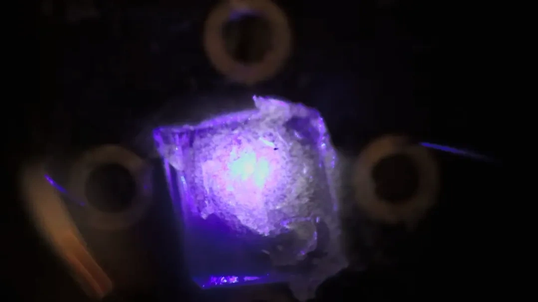
The process looks remarkably straightforward for the microchip industry. Using a premade gallium nitride wafer as the substrate, Hartensveld replaced multimillion-dollar industrial plasma-etching tools with an affordable ultraviolet laser sourced from eBay. By precisely stripping excess layers and depositing nickel, silver, and titanium contacts, he produced working blue LEDs. Adding a tiny drop of phosphor on top shifted the output to familiar daylight white. While the raw wafer was grown on commercial equipment, all high-precision lithography and microelectronic fabrication happened entirely by hand in his shed.
This garage setup will not replace mass-market consumer electronics anytime soon. However, Hartensveld’s work sets a vital benchmark for independent DIY workshops and hardware startups. The experiment proves that functional, low-volume semiconductor components for prototypes can be built without corporate budgets, paving the way for faster, cheaper custom gadget development.